「OLED Build a structure (material region setting)」:修訂間差異
跳至導覽
跳至搜尋
已建立頁面,內容為 "'''● OLED schematic structure and band diagram<br><br>''' 300px<br><br> '''● Set up the width of structure<br><br>''' You can refer to the $r..." |
無編輯摘要 |
||
| (未顯示同一使用者於中間所作的 1 次修訂) | |||
| 第1行: | 第1行: | ||
'''● | |||
'''● 2D_OLED schematic structure and band diagram<br><br>''' | |||
[[File:OLED.png|300px]]<br><br> | [[File:OLED.png|300px]]<br><br> | ||
'''● Set up the width of structure<br><br>''' | '''● Set up the width of structure<br><br>''' | ||
You can refer to the [[$ranges]] command.<br><br> | You can refer to the [[$ranges]] command.<br><br> | ||
[[File:OLED_1.png|1000px]]<br><br> | [[File:OLED_1.png|1000px]]<br><br> | ||
'''● Set up the thickness of structure<br><br>''' | '''● Set up the thickness of structure<br><br>''' | ||
Includes 5 layers of different materials and 10 virtual layers for random doping.<br><br> | Includes 5 layers of different materials and 10 virtual layers for random doping.<br><br> | ||
| 第12行: | 第15行: | ||
[[File:OLED_6.png|1000px]]<br><br> | [[File:OLED_6.png|1000px]]<br><br> | ||
[[File:OLED_7.png|1000px]]<br><br> | [[File:OLED_7.png|1000px]]<br><br> | ||
'''● Set linear contact<br><br>''' | '''● Set linear contact<br><br>''' | ||
You can refer to the [[$xd]], [[$contact]] and [[$bottomcontactnum]] commands.<br><br> | |||
[[File:OLED_8.png|1000px]]<br><br> | [[File:OLED_8.png|1000px]]<br><br> | ||
[[File:OLED_9.png|1000px]]<br><br> | [[File:OLED_9.png|1000px]]<br><br> | ||
於 2025年1月6日 (一) 14:50 的最新修訂
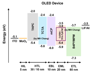
● 2D_OLED schematic structure and band diagram
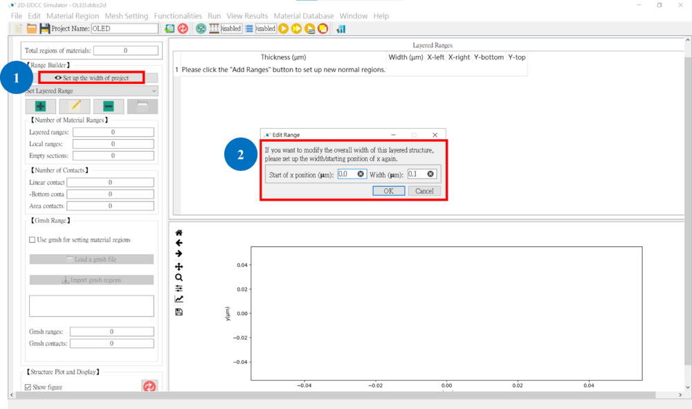
● Set up the width of structure
You can refer to the $ranges command.
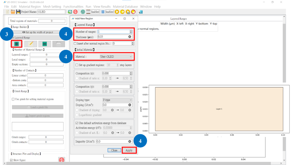
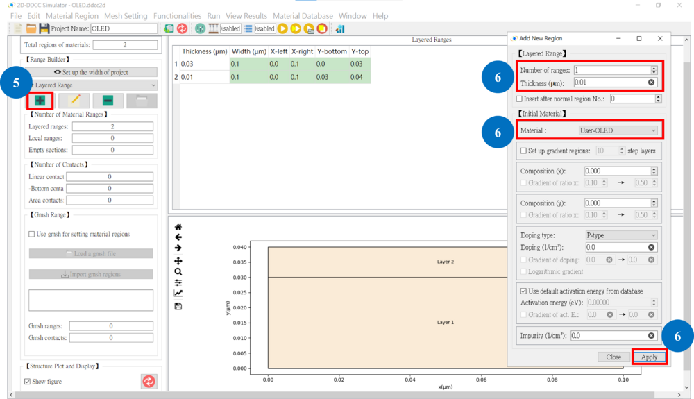
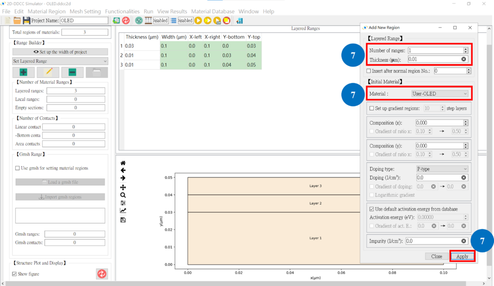
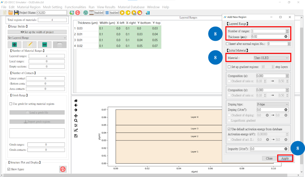
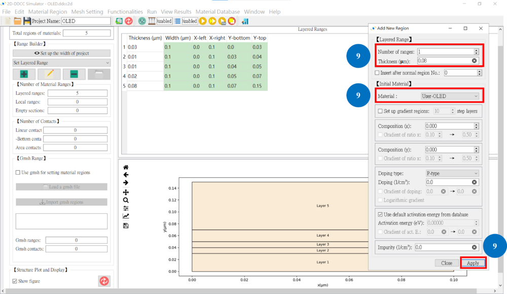
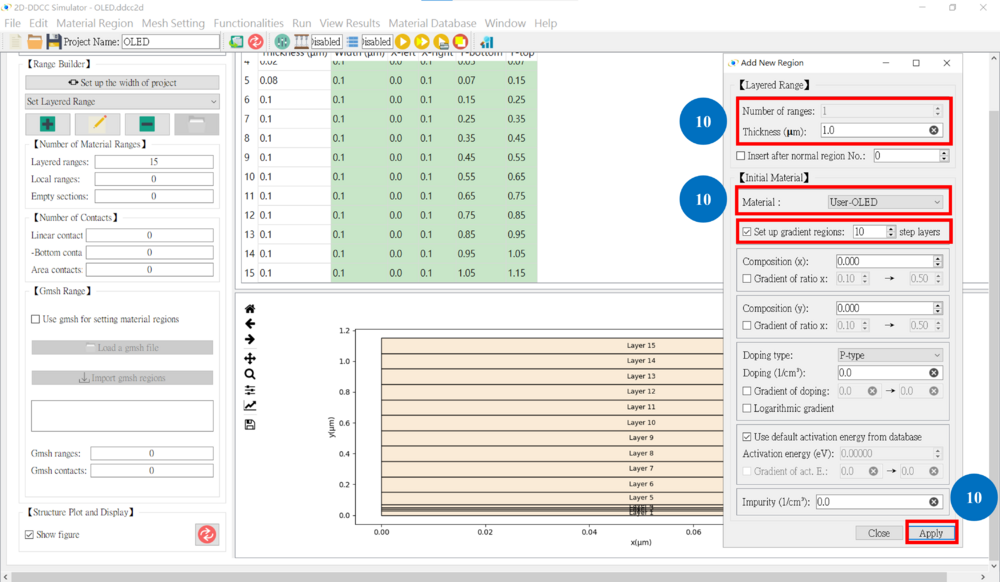
● Set up the thickness of structure
Includes 5 layers of different materials and 10 virtual layers for random doping.
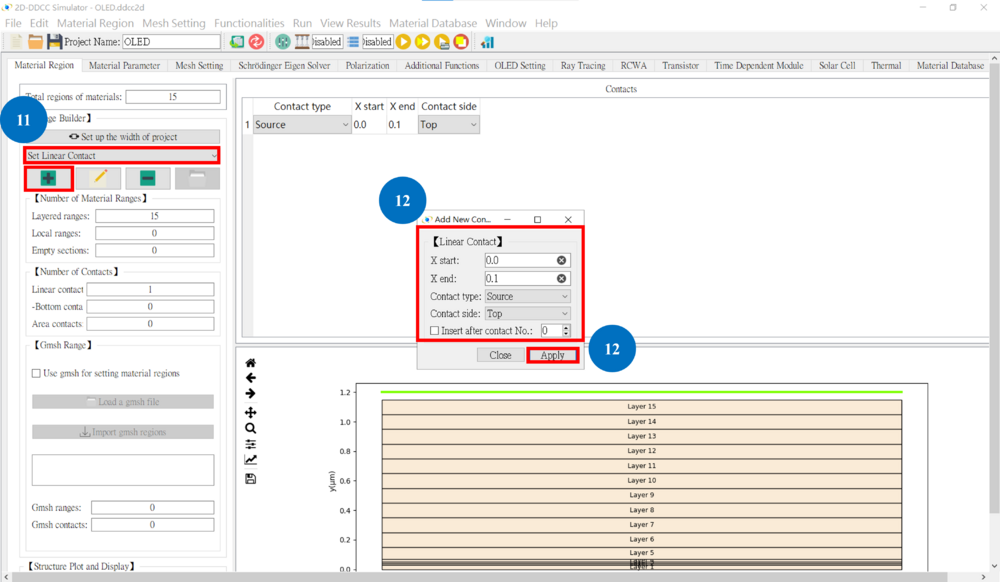
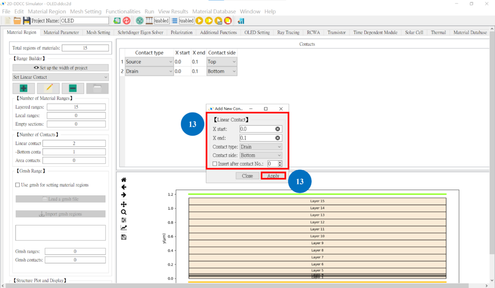
● Set linear contact
You can refer to the $xd, $contact and $bottomcontactnum commands.
