「2D HEMT View the results」:修訂間差異
無編輯摘要 |
無編輯摘要 |
||
| (未顯示同一使用者於中間所作的 3 次修訂) | |||
| 第47行: | 第47行: | ||
★ Use "hold on" to plot Ec, Ev, Efn and Efp in the same figure (along y-axis) <br><br> | ★ Use "hold on" to plot Ec, Ev, Efn and Efp in the same figure (along y-axis) <br><br> | ||
[[File:HEMT_36.png|1000px]]<br><br> | [[File:HEMT_36.png|1000px]]<br><br> | ||
'''● 2D Carrier Density figure <br><br>''' | |||
★ n (Change the logarithmic range of the z-axis)<br><br> | |||
[[File:HEMT_41.png|1000px]]<br><br> | |||
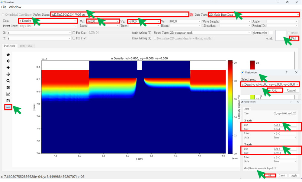
★ Change the x-axis and y-axis range for the case where Vg = -8V. <br><br> | |||
[[File:HEMT_42.png|1000px]]<br><br> | |||
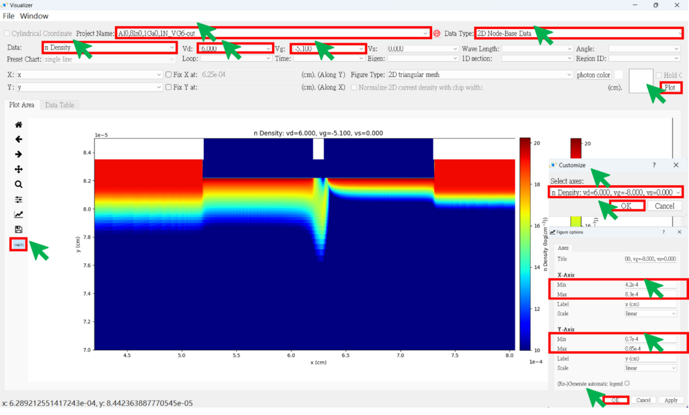
★ Change the x-axis and y-axis range for the case where Vg = -5.1V. <br><br> | |||
[[File:HEMT_43.png|1000px]]<br><br> | |||
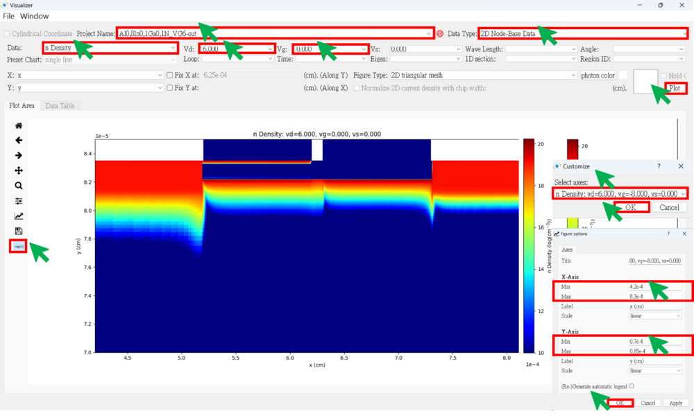
★ Change the x-axis and y-axis range for the case where Vg = 0V. <br><br> | |||
[[File:HEMT_44.png|1000px]]<br><br> | |||
'''● Parameter Check <br><br>''' | |||
You can check whether the different parameters are set correctly.<br> | |||
Ex: region number, Eg, dope, effective mass, impurity, taun(nonrad), taup(nonrad)... <br><br> | |||
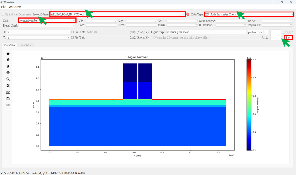
★ Region Number <br><br> | |||
[[File:HEMT_45.png|1000px]]<br><br> | |||
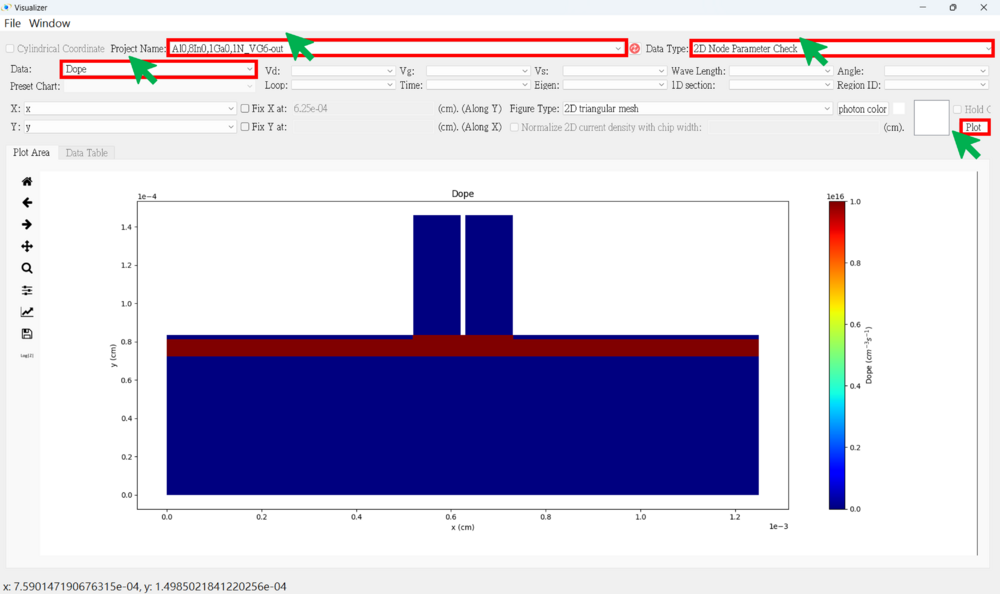
★ Dope <br><br> | |||
[[File:HEMT_46.png|1000px]]<br><br> | |||
於 2025年1月10日 (五) 09:03 的最新修訂
● Press the result viewer button
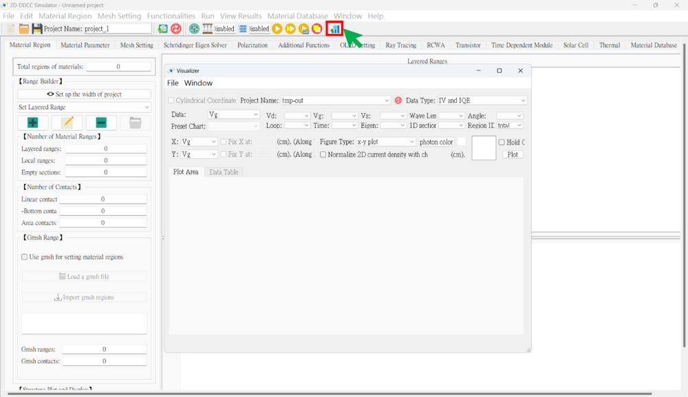
● 2D Result SOP
1. Choose the project name
2. Choose the data type
(1)  IV And IQE (Usually Use)
(2)  2D Node-Base Data (Usually Use)
(3)  2D Element-Base Data
(4)  2D Ray Tracing
(5)  2D Triangular Mesh
(6)  2D Node Parameter Check (Usually Use)
(7)  2D Element Parameter Check
(8)  2D Nsum Data
(9)  2D Eigen Wave
(10) 2D RCWA
3. Selecting voltage points (if necessary)
4. Choose the x-axis and y-axis data
5. Choose the figure type
(1)  x-y plot
     (a) Plot along the y-axis at a fixed x-point
     (b) Plot along the x-axis at a fixed y-point
(2)  2D triangular mesh
     (a) Plot the complete data for both the x-axis and y-axis
(3) 3D triangular mesh
6. Hold on (if necessary)
7. Plot
Notice: Remember to normalize the 2D current density by the chip width (cm) when plotting current data.
★★★ There are some result examples for this case. ★★★
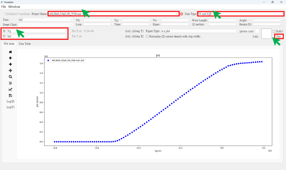
● IV figure (linear)
★ Vd_Jns
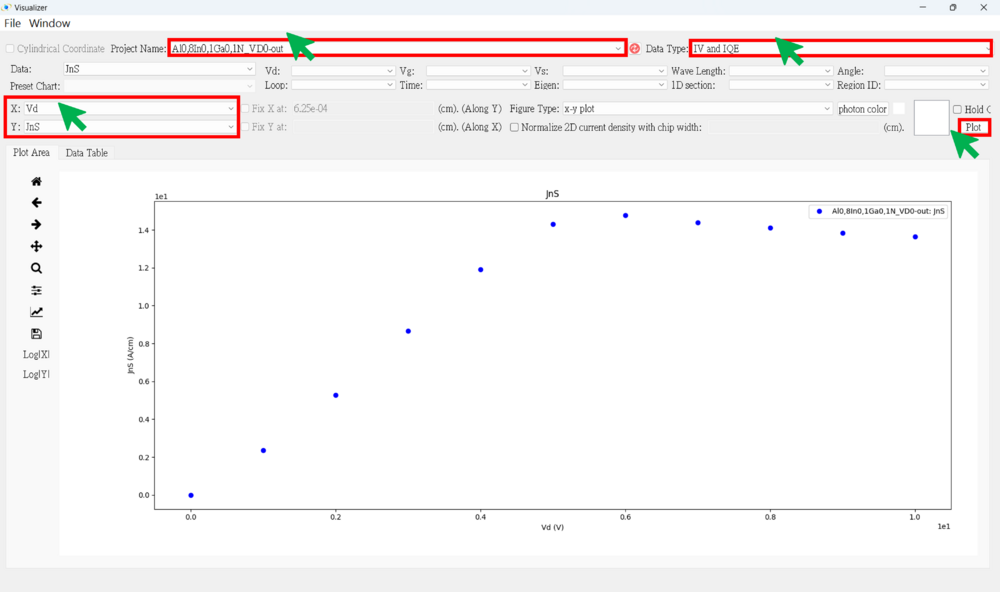
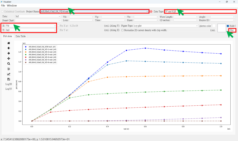
★ "Use the "hold on" command to plot curves for different drain voltages. (ex : Vd = 0, -1, -2, -3, -4, -5, -6)
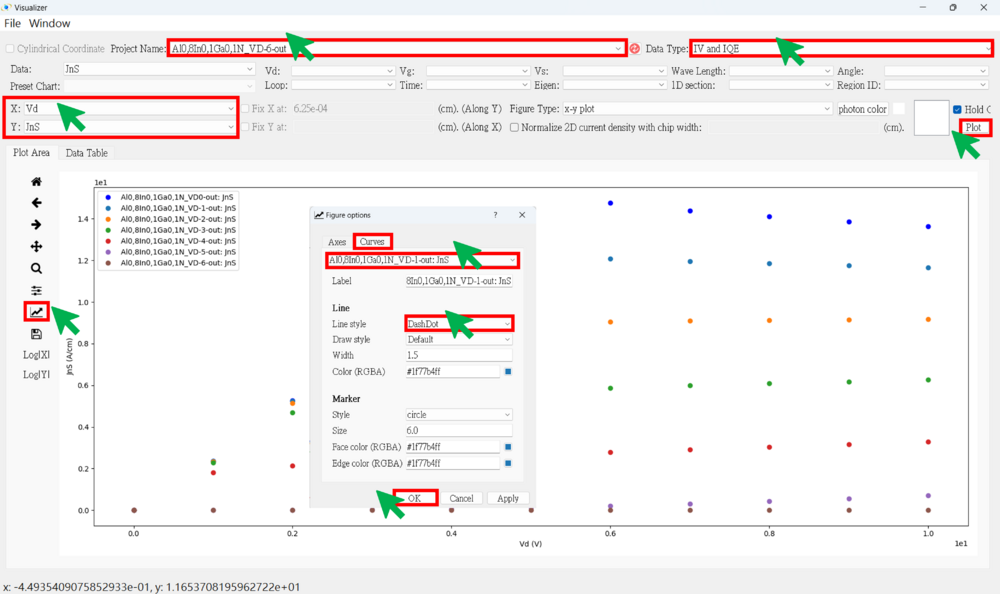
★ Change the line style of the curve.
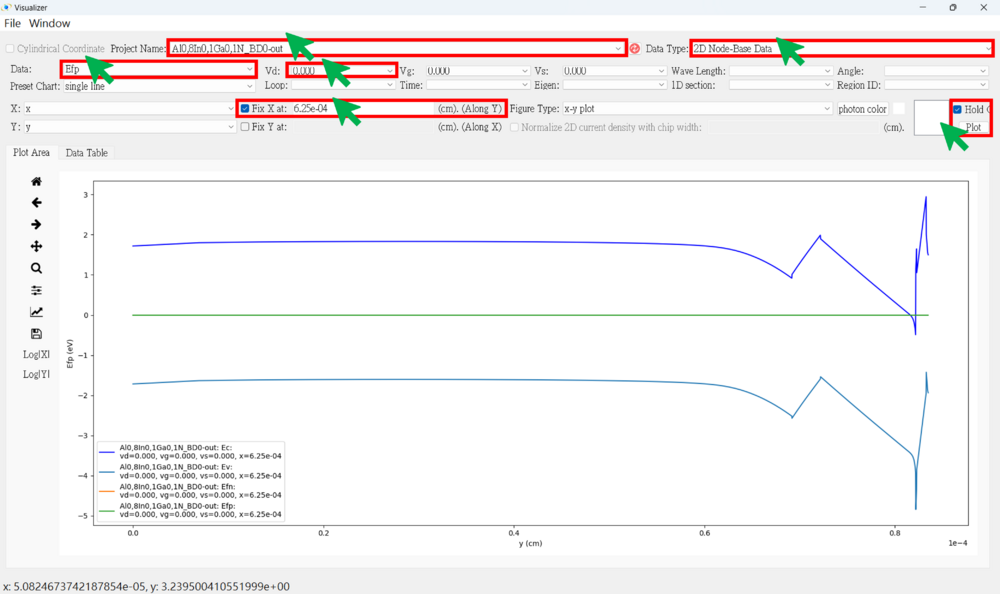
● Band stucture figure
★ Use "hold on" to plot Ec, Ev, Efn and Efp in the same figure (along y-axis)
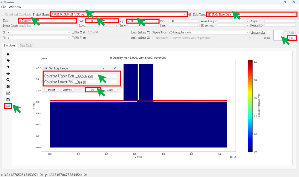
● 2D Carrier Density figure
★ n (Change the logarithmic range of the z-axis)
★ Change the x-axis and y-axis range for the case where Vg = -8V.
★ Change the x-axis and y-axis range for the case where Vg = -5.1V.
★ Change the x-axis and y-axis range for the case where Vg = 0V.
● Parameter Check
You can check whether the different parameters are set correctly.
Ex: region number, Eg, dope, effective mass, impurity, taun(nonrad), taup(nonrad)...
★ Region Number
★ Dope
