「$parameters」:修訂間差異
跳至導覽
跳至搜尋
無編輯摘要 |
小無編輯摘要 |
||
| 第50行: | 第50行: | ||
<br>'''<big><big>The $parameters setting in GUI interface is here</big></big>''' <br> | <br>'''<big><big>The $parameters setting in GUI interface is here</big></big>''' <br> | ||
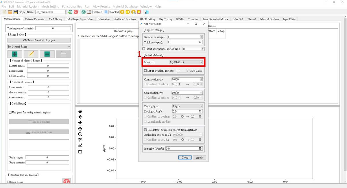
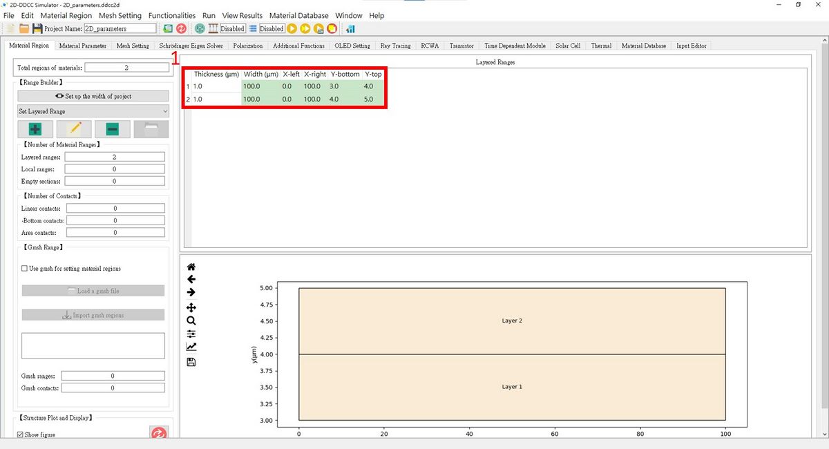
1. In this case, I chose Si as my material because the relative dielectric constant of the two layers is 11.7, as mentioned in the above example.<br> | 1. In this case, I chose Si as my material because the relative dielectric constant of the two layers is 11.7, as mentioned in the above example.<br> | ||
[[檔案:2D_parameters_fig1.jpg|1200px]]<br> | [[檔案:2D_parameters_fig1.jpg|1200px]]<br><br> | ||
[[檔案:2D_parameters_fig2.jpg|1200px]]<br> | [[檔案:2D_parameters_fig2.jpg|1200px]]<br><br> | ||
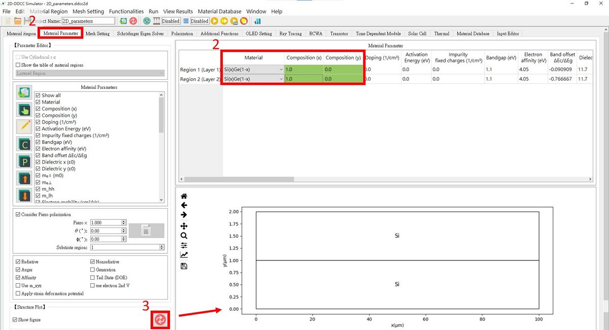
2. Press the '''Material Parameter''' and set the Composition(x) = 1, then the material become Si.<br> | 2. Press the '''Material Parameter''' and set the Composition(x) = 1, then the material become Si.<br> | ||
3. Press the '''Re-plot the depiction of material structure''' to refresh the figure!<br> | 3. Press the '''Re-plot the depiction of material structure''' to refresh the figure!<br> | ||
[[檔案:2D_parameters_fig3.jpg|1200px]]<br><br> | |||
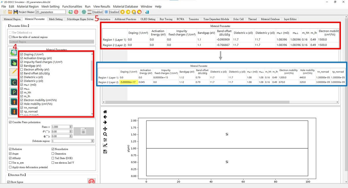
4. To show it more clearly, I ticked off the 15 parameters we need.<br> | 4. To show it more clearly, I ticked off the 15 parameters we need.<br> | ||
5. Now, fill in the table for Material Parameters, similar to the blue box!<br> | 5. Now, fill in the table for Material Parameters, similar to the blue box!<br> | ||
[[檔案:2D_parameters_fig4.jpg|1200px]]<br> | [[檔案:2D_parameters_fig4.jpg|1200px]]<br> | ||
於 2024年8月22日 (四) 10:37 的修訂
Function to assign the related information of each layer.
Format
$parameters
dope    ea    eg    dix    diy    eoff    m0off    m0in     mhh     mlh    impurity    mun     mup     taun     taup
Parameter Explanation
- Dope : The doping concentration of the material.
- Ea : The activation energy of the material.
- Eg : The bandgap of the material.
- dix : The relative dielectric constant in x-direction.
- diy : The relative dielectric constant in y-direction.
- Eoff : The conduction iband offset of this layer and next layer.
- m0off : The parallel effective mass of electron.
- m0in : The perpendicular effective mass of electron.
- mhh : The heavy hole effective mass.
- mlh : The light hole effective mass.
- impurity : The background doping concentration.
- mun : Electron mobility.
- mup : Hole mobility.
- taun : Electron carrier lifetime.
- taup : Hole lifetime.
Example
$parameters
0.0e 00 0.000 1.12 11.7 11.7 0.79 1.08 1.08 0.16 0.49 8.0e 15 1.2e 03 4.4e 02 1.3e-05 1.3e-05 -5.0e 17 0.045 1.12 11.7 11.7 0.79 1.08 1.08 0.16 0.49 0.0e 00 6.7e 02 3.2e 02 3.0e-09 3.0e-09
The $parameters setting in GUI interface is here
1. In this case, I chose Si as my material because the relative dielectric constant of the two layers is 11.7, as mentioned in the above example.


2. Press the Material Parameter and set the Composition(x) = 1, then the material become Si.
3. Press the Re-plot the depiction of material structure to refresh the figure!

4. To show it more clearly, I ticked off the 15 parameters we need.
5. Now, fill in the table for Material Parameters, similar to the blue box!
