2D OLED View the results
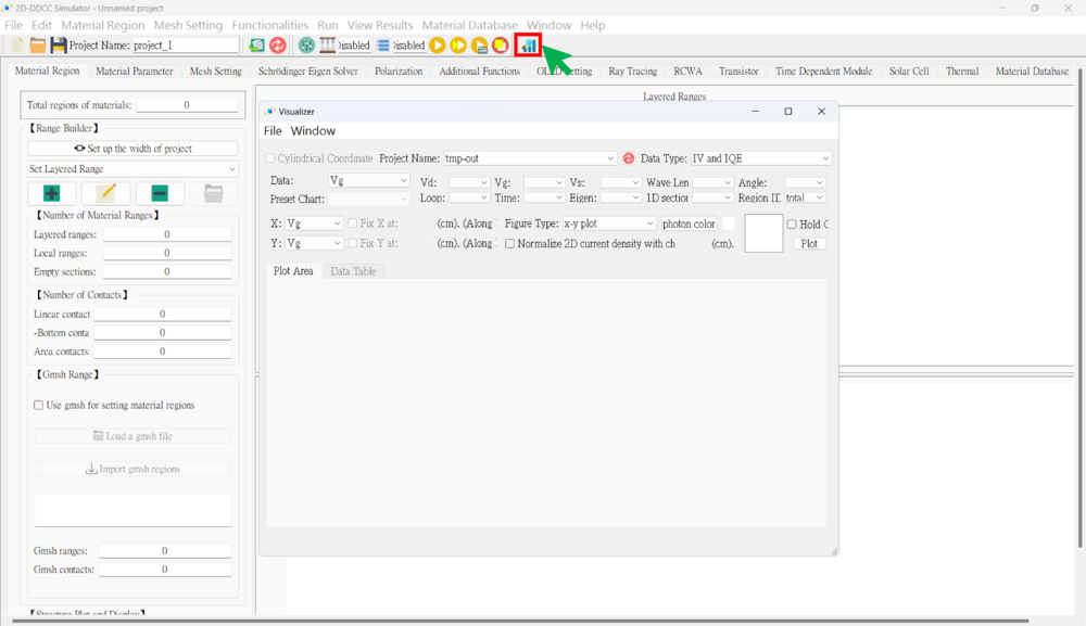
● Press the result viewer button
● 2D Result SOP
1. Choose the project name
2. Choose the data type
(1)  IV And IQE (Usually Use)
(2)  2D Node-Base Data (Usually Use)
(3)  2D Element-Base Data
(4)  2D Ray Tracing
(5)  2D Triangular Mesh
(6)  2D Node Parameter Check (Usually Use)
(7)  2D Element Parameter Check
(8)  2D Nsum Data
(9)  2D Eigen Wave
(10) 2D RCWA
3. Selecting voltage points (if necessary)
4. Choose the x-axis and y-axis data
5. Choose the figure type
(1)  x-y plot
     (a) Plot along the y-axis at a fixed x-point
     (b) Plot along the x-axis at a fixed y-point
(2)  2D triangular mesh
     (a) Plot the complete data for both the x-axis and y-axis
(3) 3D triangular mesh
6. Hold on (if necessary)
7. Plot
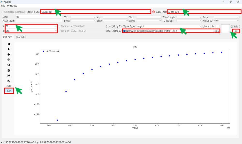
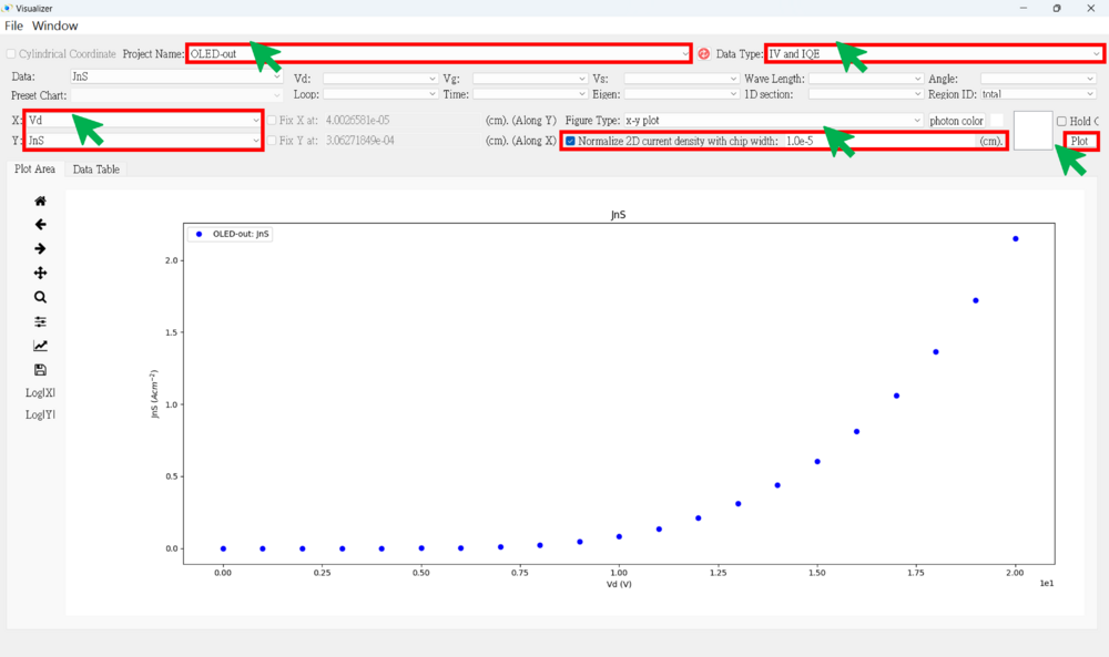
Notice: Remember to normalize the 2D current density by the chip width (cm) when plotting current data.
★★★ There are some result examples for this case. ★★★
● IV figure (linear)
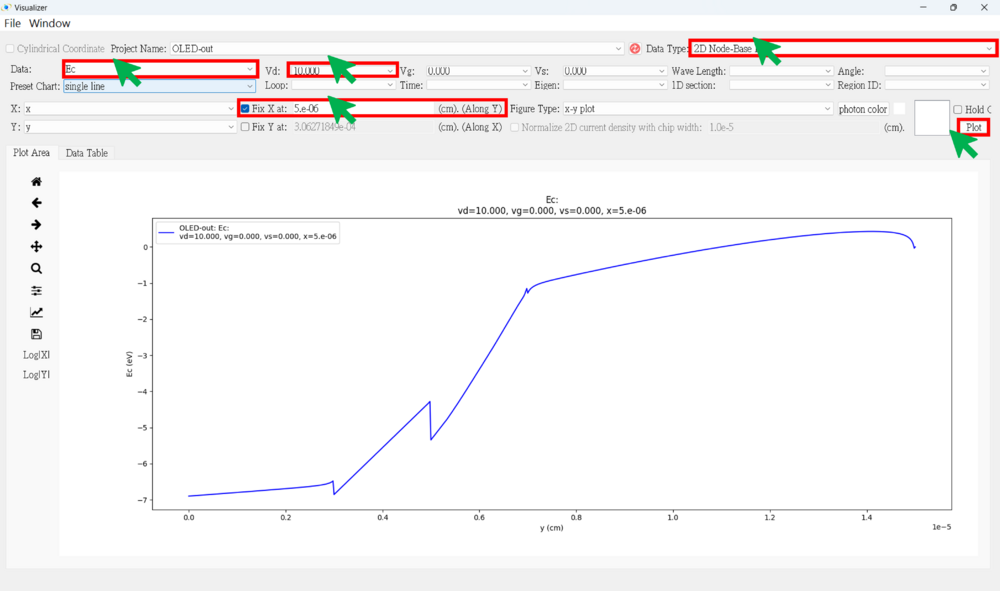
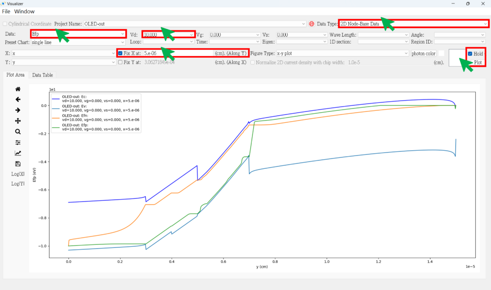
● Band structure figure
★ Ec (along y-axis)
★ Use "hold on" to plot Ec, Ev, Efn and Efp in the same figure (along y-axis)
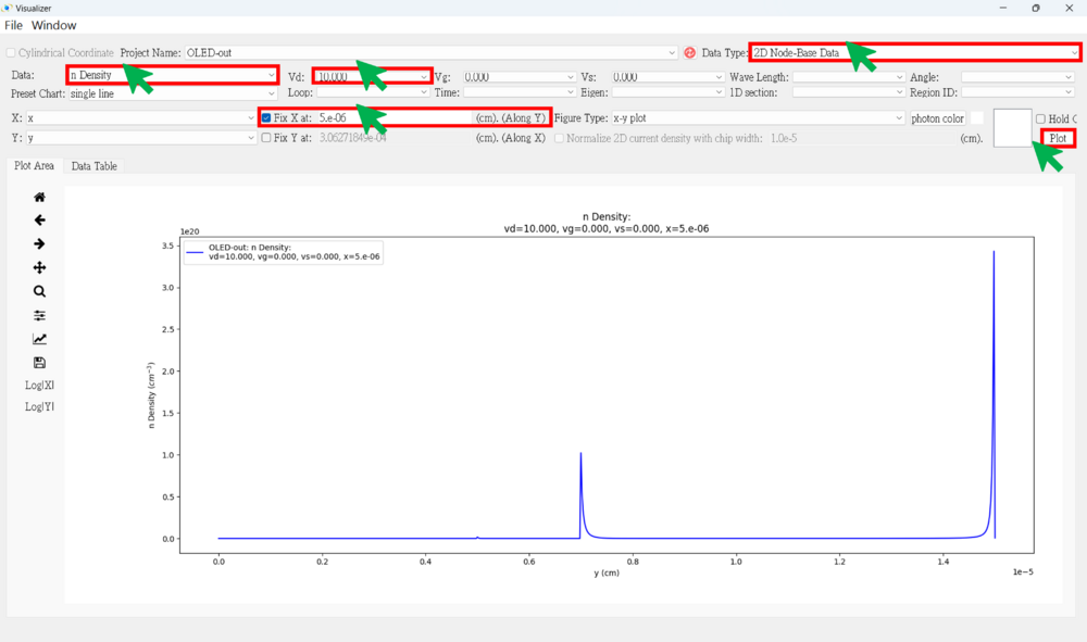
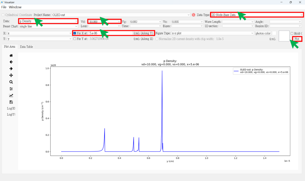
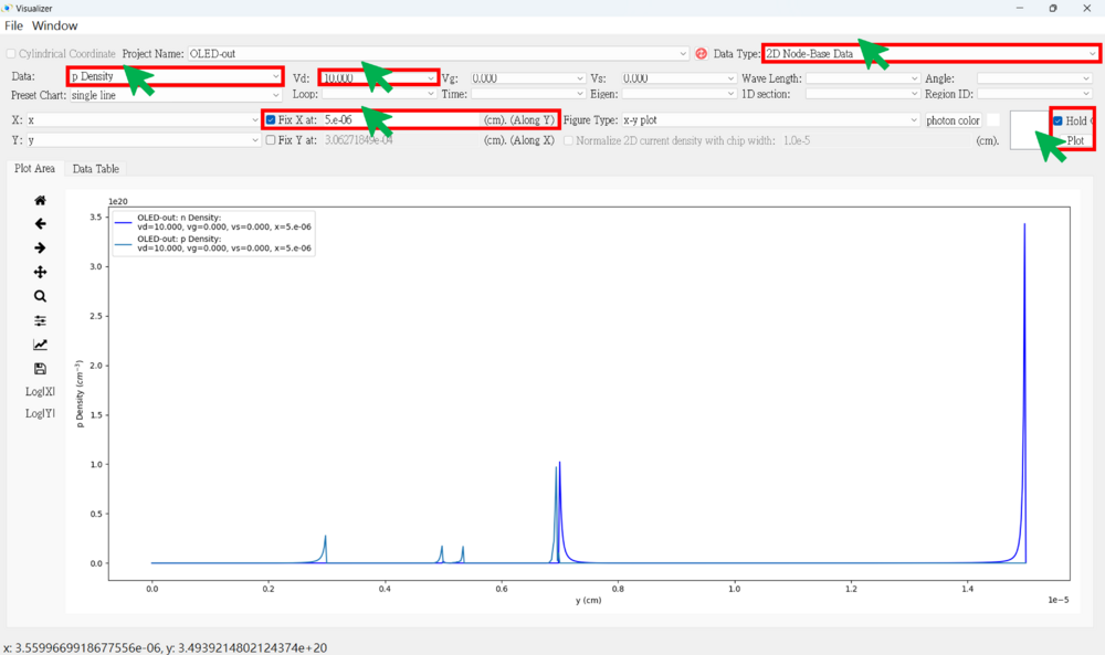
● Carreir Density figure (along y-axis)
★ n
★ p
★ Use "hold on" to plot n and p density in the same figure (along y-axis)
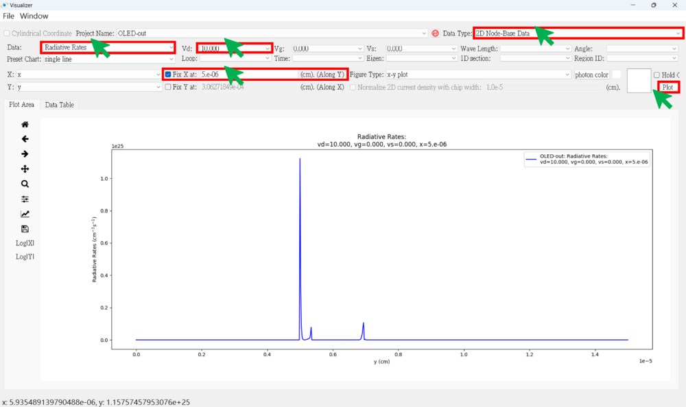
● Radiative Rates figure (along y-axis)
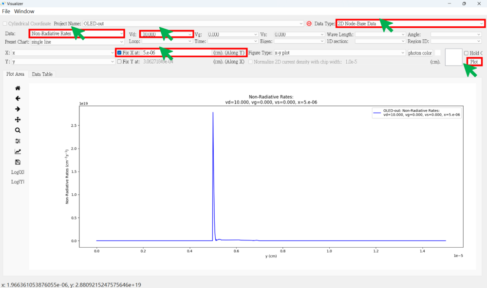
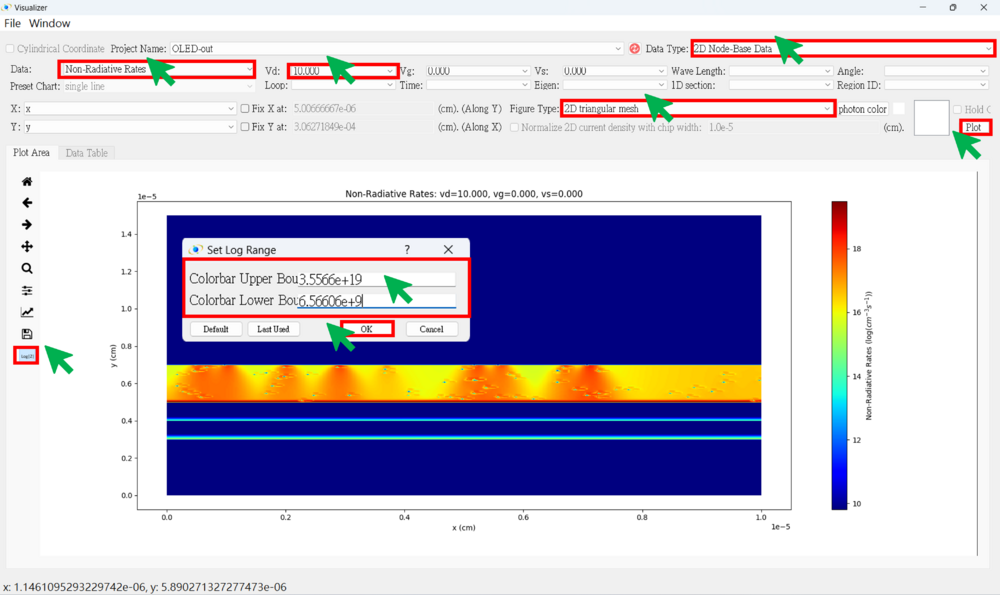
● Non-Radiative Rates figure (along y-axis)
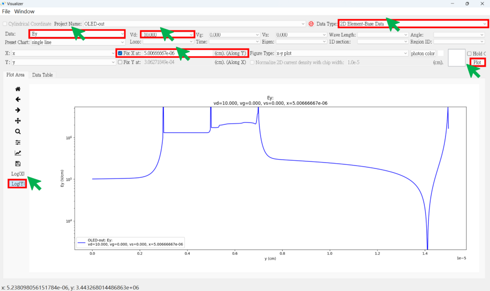
● Electric Field figure (along y-axis)
★ Ey (log)
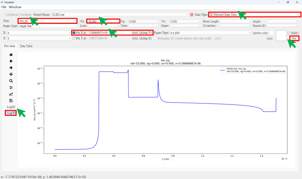
● Mobility figure (along y-axis)
★ mu_ny (log)
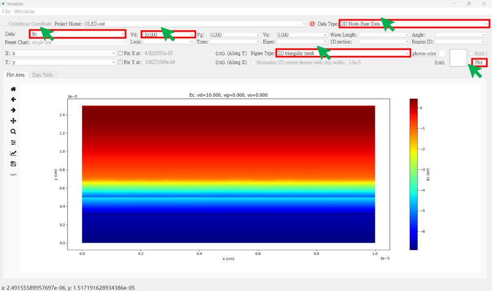
● 2D Band Structure figure
★ Ec
★ Ev
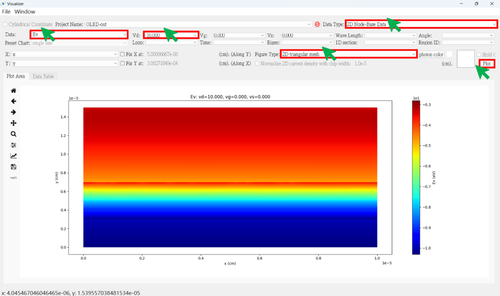
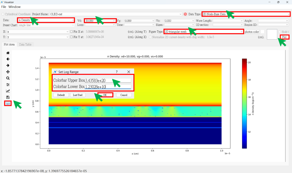
● 2D Carrier Density figure (adjust the logz range)
★ n
★ p
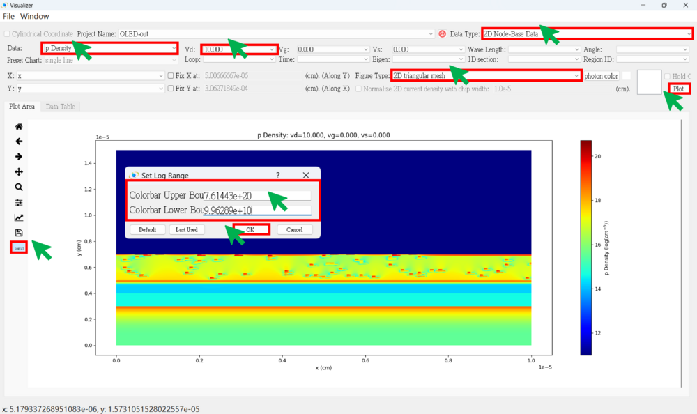
● 2D Radiative Rates figure (adjust the logz range)
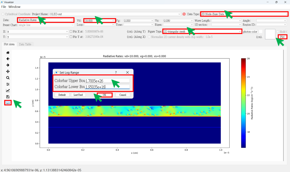
● 2D Non-Radiative Rates figure (adjust the logz range)
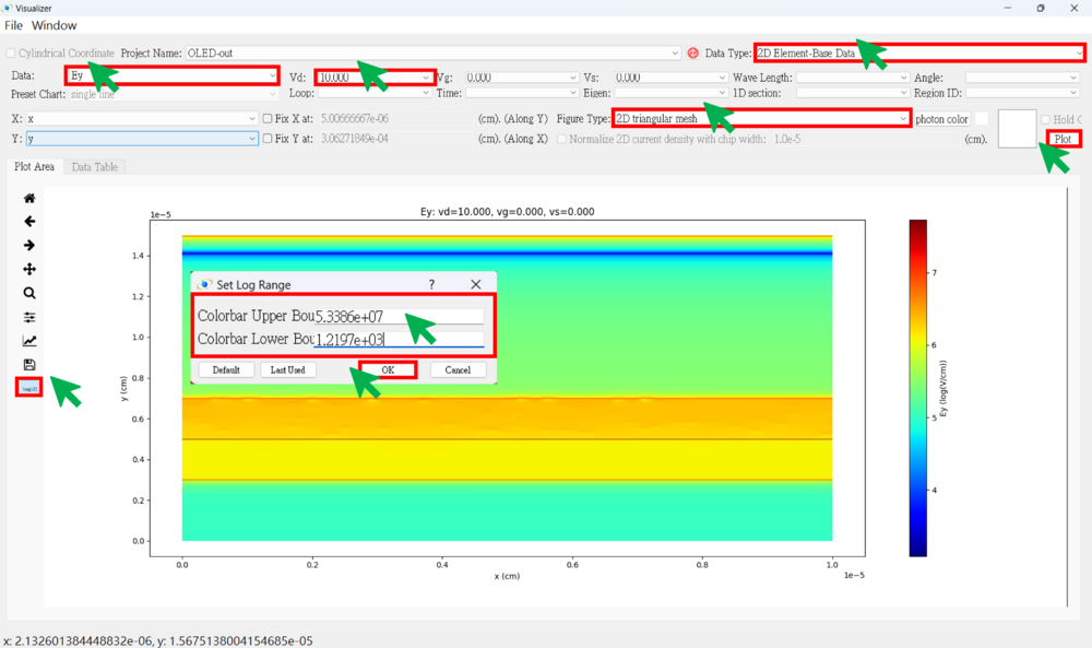
● 2D Electric Field figure (adjust the logz range)
★ Ey
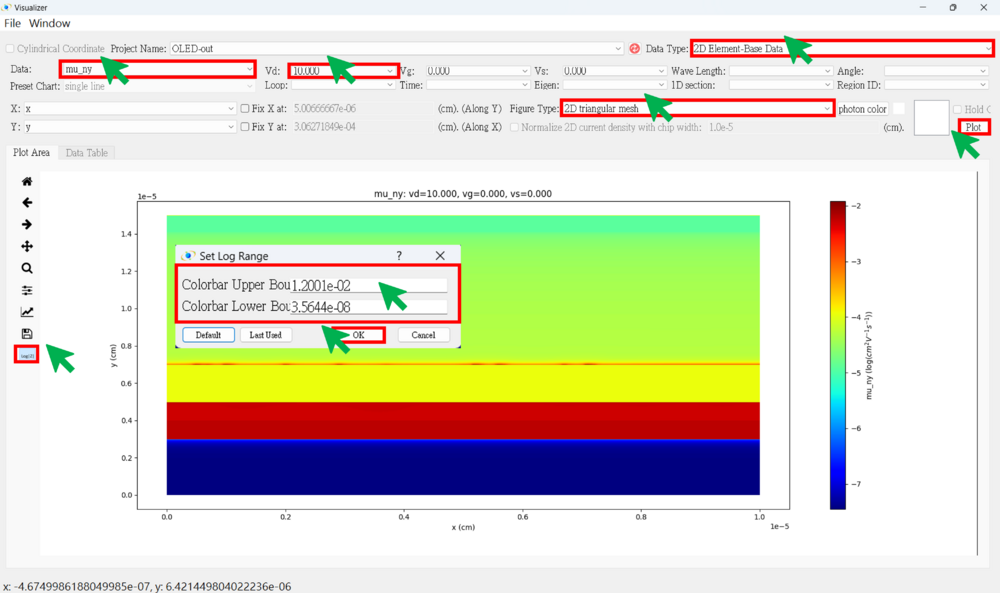
● 2D Mobility figure (adjust the logz range)
★ mu_ny
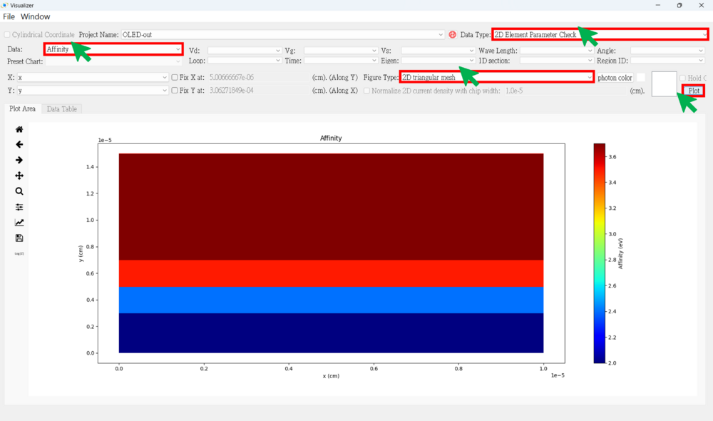
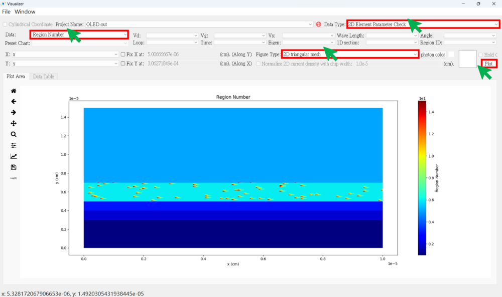
● Parameter Check
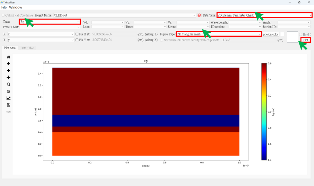
You can check whether the different parameters are set correctly.
Ex: region number, Eg, dope, effective mass, impurity, taun(nonrad), taup(nonrad)...
★ Region Number (Region numbers greater than 6 correspond to the guest material.)
★ Eg
★ Affinity
