2D LED View the results
● Press the result viewer button
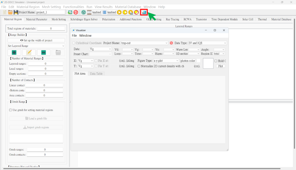
● 2D Result SOP
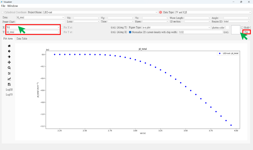
1. Choose the project name
2. Choose the data type
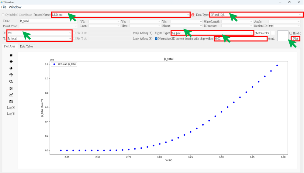
(1)  IV And IQE (Usually Use)
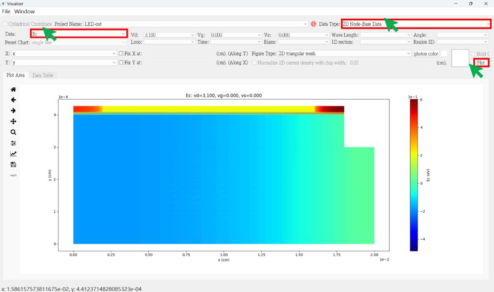
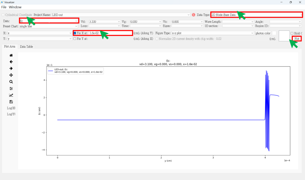
(2)  2D Node-Base Data (Usually Use)
(3)  2D Element-Base Data
(4)  2D Ray Tracing
(5)  2D Triangular Mesh
(6)  2D Node Parameter Check (Usually Use)
(7)  2D Element Parameter Check
(8)  2D Nsum Data
(9)  2D Eigen Wave
(10) 2D RCWA
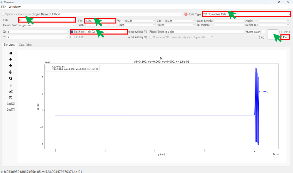
3. Choose the x-axis and y-axis data
4. Choose the figure type
(1)  x-y plot
(2)  2D triangular mesh
     (a) Plot the complete data for both the x-axis and y-axis
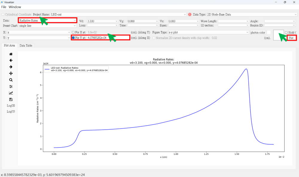
     (b) Plot along the y-axis at a fixed x-point
     (c) Plot along the x-axis at a fixed y-point
(3)  3D triangular mesh
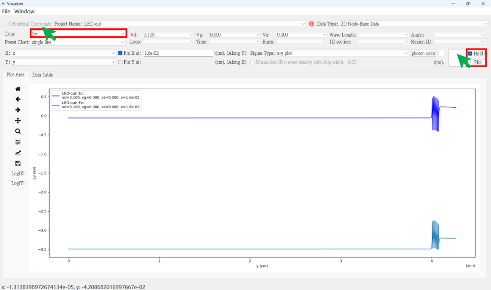
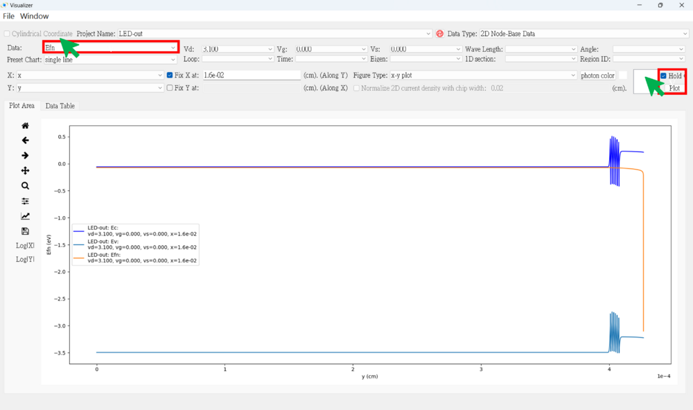
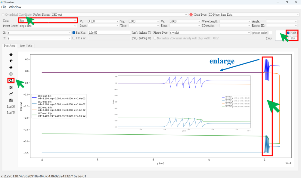
5. Hold on (if necessary)
6. Plot
Notice: Remember to normalize the 2D current density by the chip width (cm) when plotting current data.
● IV figure (log|y|) → positive current
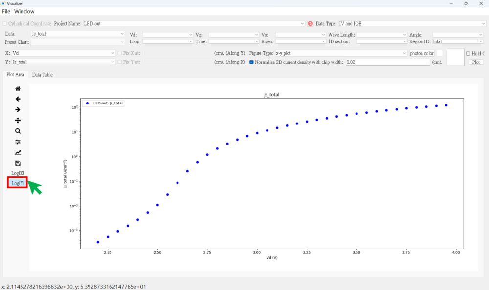
● IV figure (log|y|) → negative current
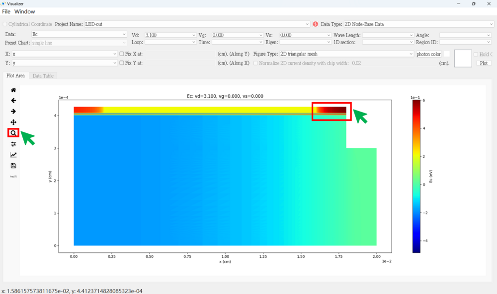
● Band structure figure
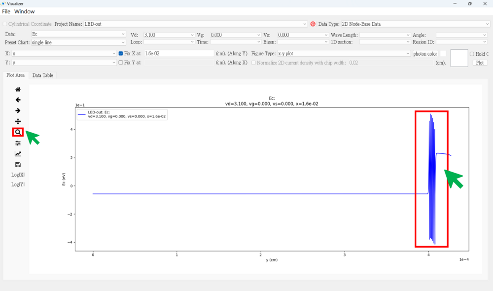
★ Ec (along y-axis)
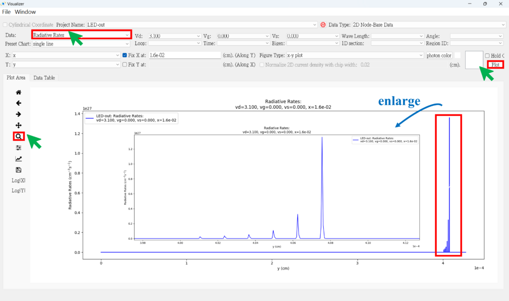
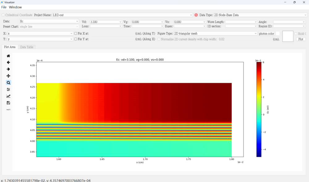
Then, enlarge a part of quantum well region.
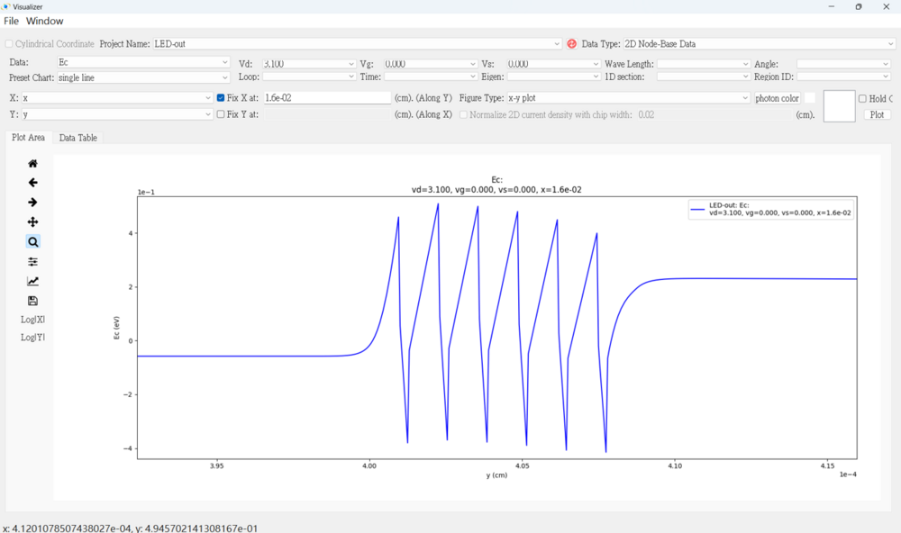
★ Use "hold on" to plot Ec, Ev, Efn, and Efp in the same figure (along y-axis)
● Radiative Rates figure (along y-axis)
